
Table of Contents
- Executive Summary: 2025 and Beyond for Angstrom-Scale Nanogap Fabrication
- Market Landscape: Current Size, Growth, and 2029 Forecast
- Core Technologies: State-of-the-Art Nanogap Fabrication Methods
- Key Industry Players and Official Developments
- Emerging Applications: Quantum Computing, Biosensing, and Nanoelectronics
- Material Innovations and Manufacturing Challenges
- Intellectual Property and Regulatory Considerations
- Strategic Partnerships and Global Supply Chain Insights
- Investment Trends and Funding Outlook (2025–2029)
- Future Opportunities and Disruptive Trends in Angstrom-Scale Nanogap Technology
- Sources & References
Executive Summary: 2025 and Beyond for Angstrom-Scale Nanogap Fabrication
The field of angstrom-scale nanogap fabrication is entering a pivotal phase in 2025, driven by the relentless demand for miniaturization in electronics, quantum devices, and sensing technologies. Recent advancements have been propelled by both academic breakthroughs and the industrial scaling of novel nanofabrication techniques. The current trajectory suggests that, over the next few years, angstrom-scale precision will shift from proof-of-concept demonstrations to broader deployment in commercial applications.
Key technology providers and semiconductor manufacturers are investing significantly in advanced lithographic and etching processes. ASML has continued to refine its extreme ultraviolet (EUV) lithography systems, now capable of sub-10 nm patterning and enabling further reductions towards the angstrom regime. Simultaneously, Lam Research is introducing atomic layer etching (ALE) solutions, which provide atomic-level precision required for fabricating ultra-narrow nanogaps in both logic and memory devices.
Materials engineering companies are also playing a significant role. Applied Materials has launched new process modules that combine atomic layer deposition (ALD) and atomic layer etch in integrated platforms, supporting the controlled creation of gaps below 1 nm. These toolsets are crucial for the fabrication of next-generation transistors and interconnects, especially as device architectures become three-dimensional and more complex.
Collaborations between industry and leading research institutes, such as the partnership between TSMC and global equipment suppliers, are accelerating the transition of angstrom-scale processes from laboratory-scale to high-volume manufacturing. This is particularly evident in the development of gate-all-around (GAA) FETs and advanced tunneling devices, where sub-nanometer gaps are essential for performance and energy efficiency.
Looking ahead, the commercialization outlook for angstrom-scale nanogap technologies is promising. The International Roadmap for Devices and Systems (IRDS), coordinated by IEEE, forecasts that mass production of devices with angstrom-scale features will be feasible within the next three to five years. The primary challenges remain in yield optimization, defect control, and metrology at such small dimensions, but ongoing investments by companies like KLA in advanced inspection and measurement tools are expected to address these hurdles.
In summary, 2025 marks a transitional year where angstrom-scale nanogap fabrication is moving from early adoption to broader commercialization, underpinned by robust industrial investment, cross-sector collaboration, and rapid technology maturation. The next few years will likely witness the integration of these ultra-fine features into mainstream semiconductor and quantum technologies.
Market Landscape: Current Size, Growth, and 2029 Forecast
The global market for angstrom-scale nanogap fabrication technologies is rapidly evolving in 2025, driven by breakthroughs in nanoelectronics, quantum computing, and advanced sensor development. Nanogaps—sub-nanometer to a few nanometers in width—are enabling unprecedented device miniaturization and new functionalities, particularly in single-molecule detection, tunneling devices, and ultra-high-density memory.
As of 2025, leading semiconductor and nanotechnology firms, such as ASML, are investing significantly in advanced lithography and patterning tools capable of producing features at the angstrom scale. Extreme ultraviolet (EUV) lithography, pioneered and commercialized by ASML, is central to these advancements, with next-generation high-NA EUV systems targeting sub-10 nm patterning and pushing boundaries towards the angstrom realm. Meanwhile, JEOL Ltd. and Hitachi High-Tech continue to advance electron beam lithography (EBL) and focused ion beam (FIB) systems, which are now routinely achieving nanogap dimensions below 2 nm in research and pilot production.
- Market Size (2025): While precise figures are challenging due to the sector’s nascent and cross-disciplinary nature, the broader nanofabrication equipment market, a key enabler, is valued in the tens of billions of US dollars in 2025, with angstrom-scale applications representing a fast-growing sub-segment. ASML reported continued double-digit revenue growth year-over-year in its advanced lithography segment during Q1 2025, citing strong demand from logic and memory customers targeting next-generation nodes.
- Growth Drivers: Expansion in end-use domains like quantum computing (where IBM and Intel are pursuing quantum dot and single-electron transistor architectures) and advanced biosensors (with companies such as Oxford Instruments providing enabling fabrication solutions) is accelerating adoption.
- 2029 Outlook: By 2029, the angstrom-scale nanogap segment is projected to outpace broader nanofabrication growth rates, driven by high-value applications in quantum circuitry, neuromorphic computing, and single-molecule analytics. Equipment manufacturers, including JEOL Ltd. and Hitachi High-Tech, are expected to introduce further refined EBL/FIB systems with improved throughput and reproducibility at angstrom-scale resolutions.
Overall, the angstrom-scale nanogap fabrication technology market in 2025 is characterized by robust growth, ongoing innovation, and significant investments from key players in the semiconductor, quantum, and nanoscale instrumentation industries. This trajectory is set to accelerate into the latter part of the decade as performance requirements and miniaturization demands intensify.
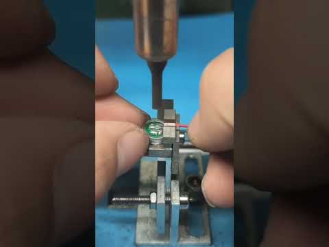
Core Technologies: State-of-the-Art Nanogap Fabrication Methods
The drive towards angstrom-scale nanogap fabrication is intensifying as applications in quantum electronics, single-molecule sensing, and next-generation transistors demand ever-smaller feature sizes. In 2025, several core technologies are emerging and maturing to enable reliable, scalable, and reproducible creation of electrode gaps below 1 nm. These include advanced lithographic techniques, self-aligned assembly, atomic layer etching, and precision mechanical break junction methods.
Electron beam lithography (EBL) and focused ion beam (FIB) milling continue to be foundational for defining nanogaps, with recent advances in beam precision and resist materials enabling sub-nanometer resolution. Companies such as JEOL Ltd. and Thermo Fisher Scientific have introduced EBL and FIB systems capable of sub-nanometer patterning, supporting research into quantum point contacts and single-molecule devices. However, throughput and cost remain challenges for large-scale manufacturing.
Self-aligned fabrication methods, particularly those leveraging bottom-up assembly, are gaining traction for their ability to achieve atomic-scale precision. For instance, the use of molecular spacers or self-assembled monolayers allows for controlled definition of nanogaps between metallic electrodes. imec has demonstrated integration of self-assembled nanogap structures within CMOS-compatible processes as part of their research into atomic-scale interconnects.
Atomic layer etching (ALE) and atomic layer deposition (ALD) are being refined to achieve atomic-scale control over material removal and addition, respectively. Lam Research Corporation and Applied Materials, Inc. are advancing ALE and ALD tools that enable precise adjustment of gap widths, addressing the need for repeatability and integration into semiconductor manufacturing lines.
Mechanically controlled break junction (MCBJ) techniques, while traditionally used in laboratory settings, are being adapted for greater stability and automation. Companies such as attocube systems AG provide piezo-driven nanopositioners that enable reliable and repeatable formation of sub-nanometer gaps under ambient or cryogenic conditions. This is particularly relevant for single-molecule electronics and quantum transport experiments.
Looking ahead, the convergence of these technologies is expected to yield nanogap fabrication platforms suitable for pilot and early commercial deployment by 2026–2028. The main challenges include ensuring uniformity over large wafer areas, reducing defect rates, and scaling up throughput. Collaborative industry-academic efforts, such as those fostered by SEMI, are anticipated to accelerate standardization and adoption, paving the way for new device architectures enabled by angstrom-scale gaps.
Key Industry Players and Official Developments
Advancements in angstrom-scale nanogap fabrication remain at the forefront of nanotechnology and semiconductor research, with several industry leaders and specialized firms driving innovation into 2025 and beyond. Angstrom-scale gaps—less than a nanometer—are critical for next-generation applications including quantum tunneling devices, single-molecule detection, and ultrafast electronics. The push for ever-smaller features has spurred official collaborations, product launches, and investments among materials suppliers, equipment manufacturers, and semiconductor foundries.
- ASML continues to dominate the field of extreme ultraviolet (EUV) lithography, a technology indispensable for sub-1 nm feature definition. In 2024 and into 2025, ASML has announced further enhancements to its High-NA EUV systems, enabling patterning precision necessary for fabrication of angstrom-scale gaps in advanced logic and memory devices.
- Tokyo Electron Limited (TEL) and Applied Materials are expanding their portfolios of atomic layer deposition (ALD) and etching systems. Both companies have introduced ALD tools capable of atomic-scale thickness control, which is critical for constructing the electrodes and isolation layers that define nanogaps. Tokyo Electron Limited’s latest ALD platforms and Applied Materials’ selective etch solutions are being adopted by logic and memory fabs targeting sub-nanometer geometries.
- Lam Research has announced next-generation atomic layer etching (ALE) equipment, which, according to the company’s 2024 and 2025 product updates, allows atomic-level precision in material removal—essential for producing consistent, reproducible angstrom-scale gaps for device interconnects (Lam Research).
- IMEC, a leading nanoelectronics research institute, is collaborating with major semiconductor manufacturers to demonstrate scalable processes for angstrom-scale gap formation. In 2025, IMEC is piloting integration of advanced self-assembly and direct-write techniques, aiming at high-throughput production for sub-1 nm quantum and biosensor devices.
- Oxford Instruments has released new atomic layer deposition and etching tools tailored for research and early-stage production of nanodevices with sub-nanometer gaps. Their official product documentation highlights partnerships with academic and commercial research centers globally (Oxford Instruments).
Looking forward, industry leaders are focused on combining advanced lithography, atomic-scale deposition/etching, and molecular self-assembly to overcome the material and process challenges of routine angstrom-gap fabrication. The next few years are expected to witness pilot lines and early commercial adoption in quantum computing, nanoscale sensors, and ultimately mainstream semiconductor manufacturing.
Emerging Applications: Quantum Computing, Biosensing, and Nanoelectronics
The rapid advancement of angstrom-scale nanogap fabrication technologies is significantly impacting emerging fields such as quantum computing, biosensing, and nanoelectronics. In 2025, industry and academic laboratories are reporting promising breakthroughs that promise to redefine device performance and enable entirely new applications.
In quantum computing, angstrom-scale nanogaps are crucial for the creation of single-electron transistors, qubit control elements, and quantum tunneling devices. Companies like IBM and Intel Corporation are actively exploring atomic-precision fabrication methods, such as scanning tunneling microscopy (STM) lithography and advanced e-beam patterning, to create contacts and gate structures with sub-nanometer separations. These approaches are essential for controlling electron tunneling and coherence in quantum devices, which operate at the limits of material and geometric precision. In 2025, IBM announced successful integration of angstrom-scale features in prototype quantum circuits, leading to improved device fidelity and scaling prospects.
For biosensing, angstrom-scale nanogaps enable the direct electrical detection of single molecules and biomolecular interactions. Companies such as Oxford Nanopore Technologies are leveraging solid-state nanopore devices with sub-nanometer gap control to achieve unprecedented sensitivity in DNA and protein sensing. Recent advances involve the use of atomic layer deposition (ALD) and controlled electromigration techniques to reliably fabricate these gaps at scale. In 2025, Oxford Nanopore Technologies reported commercial deployment of angstrom-scale nanopore arrays, offering faster and more accurate biomolecule analysis for genomics and diagnostics.
In nanoelectronics, shrinking device features to the angstrom regime is pushing the boundaries of Moore’s Law. Taiwan Semiconductor Manufacturing Company (TSMC) and Samsung Electronics are both investing in novel processes such as selective atomic layer etching and self-aligned patterning to create transistor gate lengths and interconnects below one nanometer. These innovations, anticipated to reach pilot manufacturing in 2025-2026, are expected to deliver substantial improvements in device performance, energy efficiency, and integration density.
Looking forward, the convergence of advanced nanogap fabrication with AI-driven process control, in-line metrology, and new materials is expected to accelerate commercialization. Collaborations between manufacturers, tool providers, and research institutions will likely yield scalable production techniques for angstrom-scale gaps, opening pathways to next-generation quantum processors, ultra-sensitive biosensors, and ultra-dense logic circuits.
Material Innovations and Manufacturing Challenges
The pursuit of angstrom-scale nanogap fabrication—where electrode separations approach sub-nanometer dimensions—has become a focal point in nanoelectronics, quantum computing interfaces, and molecular sensing technologies. This trend is driven by the need for ultra-miniaturization, single-molecule detection, and the development of next-generation quantum devices. However, transitioning from laboratory-scale demonstrations to reliable, scalable manufacturing of angstrom-scale nanogaps presents formidable material and process challenges.
In 2025, several leading materials companies and semiconductor foundries are advancing the state of nanogap technology through innovations in both materials and process integration. For example, Applied Materials is actively developing atomic layer deposition (ALD) and atomic layer etching (ALE) techniques. These approaches enable atomic-scale control over material addition and removal, which is critical for fabricating electrodes separated by just a few angstroms. Similarly, Lam Research is optimizing plasma-based etching and selective deposition technologies to achieve atomic precision in pattern transfer and gap definition, aiming to reduce variability and defect rates at these scales.
Material selection remains central to overcoming electromigration and dielectric breakdown, both of which are exacerbated at angstrom dimensions. Intel Corporation is exploring advanced interconnect metals such as cobalt and ruthenium, which offer improved stability and lower resistivity compared to traditional copper at extreme scaling. Additionally, the use of two-dimensional materials (e.g., graphene and transition metal dichalcogenides) as ultrathin spacers or electrodes is under investigation by research arms of major chipmakers and specialized nanomaterials suppliers including 2D Semiconductors.
Despite these advances, manufacturing challenges remain significant. Achieving uniformity and reproducibility across wafer-scale substrates is still limited by stochastic process variations and contamination risks. TSMC is investing in next-generation cleanroom protocols and in-line metrology capable of resolving angstrom-scale features, including advanced electron microscopy and atomic force microscopy systems. The integration of machine learning for process control is also being explored to predict and correct deviations in real time.
Looking forward to the next few years, the outlook for angstrom-scale nanogap fabrication is cautiously optimistic. While pilot demonstrations continue to emerge, high-volume manufacturing is likely to be constrained to niche applications until breakthroughs in defect control and materials reliability are achieved. Nonetheless, ongoing partnerships between equipment manufacturers, materials suppliers, and foundries are expected to accelerate innovation, bringing angstrom-scale nanogap devices closer to commercial viability by the late 2020s.
Intellectual Property and Regulatory Considerations
The rapid evolution of angstrom-scale nanogap fabrication technologies is driving significant developments in intellectual property (IP) and regulatory landscapes as we approach and enter 2025. With devices and sensors leveraging sub-nanometer gaps for applications in quantum electronics, biosensing, and next-generation memory, the race to secure foundational patents and navigate emerging standards is intensifying.
Global patent activity in this domain remains robust, with major players such as IBM, Intel Corporation, and Samsung Electronics actively filing for protections on novel fabrication methods, material systems, and integration processes. For instance, recent filings have focused on advanced lithographic techniques, self-assembly methods, and atomic layer deposition (ALD) tailored for achieving reproducible angstrom-scale features. Given the complexity of these fabrication approaches, overlapping claims and patent thickets are becoming more common, prompting industry stakeholders to pursue cross-licensing agreements and patent pools to mitigate litigation risk and foster innovation.
Regulatory considerations are also evolving alongside technological advances. As nanogap devices increasingly interface with biological systems and operate at the quantum limit, regulatory agencies are reassessing existing frameworks for device safety, environmental impact, and data integrity. Organizations such as the International Organization for Standardization (ISO) and the IEEE are actively developing standards for measurement accuracy, device reliability, and material safety in nanofabrication at the atomic scale. These efforts aim to ensure that new devices meet rigorous quality and reproducibility benchmarks, which are essential for both commercialization and regulatory approval.
In the United States, the United States Patent and Trademark Office (USPTO) has observed a year-on-year increase in filings related to angstrom-scale fabrication, reflecting the sector’s innovation intensity. Meanwhile, regulatory agencies including the Food and Drug Administration (FDA) are evaluating new guidance for nano-enabled medical devices, particularly those employing ultra-fine electrodes or biosensors, to address emerging safety and efficacy concerns.
Looking ahead, stakeholders anticipate that both the IP and regulatory environments will become more nuanced and collaborative. Efforts to harmonize international standards and clarify patentability criteria for atomic-scale inventions are expected to accelerate through 2025 and beyond, fostering a more predictable landscape for innovation and commercialization. Companies at the forefront of this field will likely continue to invest heavily in both IP generation and regulatory compliance, recognizing these as key enablers of long-term competitive advantage.
Strategic Partnerships and Global Supply Chain Insights
Strategic partnerships and robust global supply chains are pivotal for advancing angstrom-scale nanogap fabrication technologies, especially as the industry faces formidable technical and logistical challenges. In 2025, the collaborative landscape is characterized by alliances among semiconductor foundries, material suppliers, and equipment manufacturers, each contributing specialized expertise and resources to push the boundaries of miniaturization.
Leading semiconductor manufacturers such as TSMC and Intel have intensified their partnerships with equipment innovators like ASML, whose extreme ultraviolet (EUV) lithography systems are indispensable for patterning features at the sub-nanometer scale. In 2024 and 2025, these partnerships are deepening, with ASML securing multi-year supply agreements and joint technology development programs aimed at enabling high-volume production of chips with angstrom-scale features. Such collaborations are necessary not only for advancing fabrication tools but also for ensuring a steady supply of critical components, including specialized photoresists and pellicles, which are sourced from suppliers such as JSR Corporation.
Material innovation is another area benefiting from strategic collaboration. For instance, Samsung Electronics has announced joint ventures with chemical suppliers to co-develop next-generation dielectric and etching materials required for achieving reliable angstrom-scale gaps. These efforts are supported by vertically integrated supply chains, where upstream partners are embedded early in the R&D process to ensure compatibility and scalability.
On the supply chain front, the global distribution of fabrication equipment and materials remains a significant concern amid geopolitical uncertainties and ongoing disruptions. To mitigate such risks, companies like Applied Materials and Lam Research are expanding their global manufacturing footprints and establishing regional logistics hubs, particularly in North America, Europe, and East Asia. These initiatives are designed to enhance resilience and responsiveness, allowing rapid adaptation to shifting market demands and regulatory requirements.
Looking ahead, the next few years will likely see an expansion of cross-border consortia and public-private partnerships, such as those fostered by SEMI, to address talent shortages, standardization, and sustainability challenges inherent to angstrom-scale nanogap fabrication. As the ecosystem matures, closer integration of R&D, manufacturing, and supply chain management will be vital to maintaining innovation momentum and ensuring secure, reliable delivery of next-generation nanoelectronics.
Investment Trends and Funding Outlook (2025–2029)
The investment landscape for angstrom-scale nanogap fabrication technologies is poised for significant evolution through 2025 and the subsequent years. The drive toward miniaturization in semiconductor devices, quantum computing, and next-generation sensors has heightened investor interest in advanced nanofabrication methods capable of reliably producing sub-nanometer gaps.
In 2025, established industry players and specialized startups are intensifying their focus on research and development (R&D) for innovative fabrication techniques, such as atomic layer deposition, advanced electron beam lithography, and self-assembly processes. Intel Corporation has publicly committed substantial resources to scaling its process technology, emphasizing the importance of advanced patterning and etching for transistor architectures approaching the angstrom regime. Similarly, Taiwan Semiconductor Manufacturing Company (TSMC) is expanding its R&D facilities and has announced multi-billion dollar investments to advance nanoscale fabrication, including the development of processes that could enable angstrom-scale gap definition in logic and memory devices.
The funding environment is also marked by increased participation from government initiatives and research alliances. For example, the U.S. CHIPS Act and EU Chips Act have allocated significant funding to drive innovation in microelectronics manufacturing, directly benefiting organizations working on extreme miniaturization and nanogap fabrication. National laboratories and collaborative consortia—such as imec in Belgium and CSEM in Switzerland—are recipients of these public funds, enabling them to accelerate pilot projects and technology transfer to industry partners.
Venture capital (VC) and corporate venture arms are increasingly targeting deep-tech startups specializing in atomic-precision manufacturing, molecular electronics, and quantum device fabrication. Notably, Applied Materials has expanded its venture portfolio to support early-stage companies developing novel tools and materials for angstrom-scale feature formation. Similarly, Lam Research announced new innovation grants and partnerships focused on next-generation etch and deposition technologies.
Looking ahead to 2029, the sustained momentum in both private and public investment is expected to lower the barriers for commercializing angstrom-scale nanogap technologies. Industry analysts predict a gradual shift from proof-of-concept demonstrations to pilot-scale manufacturing, with leading-edge foundries integrating these capabilities into advanced nodes. The intersection of policy-driven funding, strategic corporate investments, and a vibrant startup ecosystem forms a robust foundation for continued breakthroughs in the field over the next several years.
Future Opportunities and Disruptive Trends in Angstrom-Scale Nanogap Technology
Angstrom-scale nanogap fabrication is poised to experience significant advances in 2025 and the near future, driven by the convergence of novel lithography, self-assembly, and atomic-scale manipulation techniques. As device miniaturization approaches the physical limits of silicon and quantum effects become more pronounced, angstrom-scale gaps—measured at less than one nanometer—are central to next-generation electronics, quantum computing, and ultrasensitive sensing applications.
One of the most promising developments is the emergence of advanced electron beam lithography (EBL) and focused ion beam (FIB) techniques, which are increasingly capable of patterning features well below 1 nm. Companies such as JEOL Ltd. and TESCAN continue to refine their high-resolution EBL and FIB systems, targeting sub-nanometer precision for research and early commercial processes. Complementing these, atomic layer deposition (ALD) is being leveraged to control gap dimensions at the atomic scale, with ASM International and Beneq offering process tools that enable conformal coatings with angstrom-level thickness precision.
Self-assembly and molecular templating are another area of rapid progress. Techniques such as DNA origami and molecular self-assembly are being explored to create reproducible angstrom-scale gaps, with early prototyping seen in certain nanoelectronic and biosensing applications. IBM is actively investigating bottom-up assembly methods for atomic-precision device fabrication, which could disrupt traditional top-down lithography in the coming years.
In-situ transmission electron microscopy (TEM) combined with electron-beam-induced deposition or etching is enabling real-time manipulation of nanogap structures at atomic resolution. Hitachi High-Tech Corporation and Thermo Fisher Scientific have enhanced their TEM platforms to support such advanced fabrication and metrology tasks, allowing for feedback-driven process optimization at the single-atom level.
Looking ahead, the integration of artificial intelligence (AI) and machine learning into nanogap fabrication workflows is expected to accelerate design-optimization cycles, defect prediction, and process control, as highlighted by ASML in its strategic roadmap. The next few years will likely see the first commercial devices leveraging angstrom-scale gaps for quantum tunneling transistors, single-molecule sensors, and hybrid quantum-classical systems, establishing new performance benchmarks in the semiconductor and advanced materials sectors.