Advanced Nanodevice Fabrication in 2025: Transforming Electronics and Healthcare with Breakthrough Manufacturing. Explore the Technologies, Market Dynamics, and Future Outlook Shaping the Next Era of Nano-Enabled Devices.
- Executive Summary: Key Trends and Market Drivers in 2025
- Market Size, Segmentation, and 2025–2030 Growth Forecasts
- Breakthrough Fabrication Techniques: From Atomic Layer Deposition to 3D Nanoprinting
- Material Innovations: Graphene, 2D Materials, and Beyond
- Leading Players and Strategic Partnerships (e.g., intel.com, ibm.com, imec-int.com)
- Applications: Electronics, Healthcare, Energy, and Emerging Sectors
- Regulatory Landscape and Industry Standards (e.g., ieee.org, semiconductors.org)
- Supply Chain, Manufacturing Challenges, and Solutions
- Investment Trends, M&A Activity, and Funding Outlook
- Future Outlook: Disruptive Technologies and Market Opportunities Through 2030
- Sources & References
Executive Summary: Key Trends and Market Drivers in 2025
Advanced nanodevice fabrication is poised for significant transformation in 2025, driven by rapid technological innovation, increased investment, and expanding application domains. The sector is witnessing a convergence of semiconductor miniaturization, novel materials integration, and process automation, all of which are accelerating the commercialization of next-generation nanoscale devices.
A primary trend is the continued scaling of semiconductor nodes below 3 nanometers, with leading manufacturers such as Taiwan Semiconductor Manufacturing Company (TSMC) and Samsung Electronics ramping up production of advanced logic chips. These companies are leveraging extreme ultraviolet (EUV) lithography and new transistor architectures, such as gate-all-around (GAA) FETs, to push the boundaries of device density and performance. In 2025, TSMC and Samsung are both expected to expand their 2nm pilot lines, with commercial volumes anticipated by 2026.
Material innovation is another key driver. The integration of two-dimensional materials, including graphene and transition metal dichalcogenides, is moving from research labs to pilot-scale fabrication. IBM and Intel Corporation are actively exploring these materials for high-mobility channels and ultra-low-power devices, aiming to overcome the limitations of traditional silicon. Additionally, the adoption of advanced dielectrics and novel interconnects is enabling further scaling and improved device reliability.
Process automation and digitalization are reshaping nanodevice manufacturing. Equipment suppliers such as ASML Holding and Lam Research Corporation are deploying AI-driven process control and in-line metrology, enhancing yield and reducing defectivity at the nanoscale. These advancements are critical as device complexity increases and tolerances tighten.
The market outlook for advanced nanodevice fabrication remains robust. Demand is fueled by applications in artificial intelligence, high-performance computing, 5G/6G communications, and emerging quantum technologies. Strategic investments by governments and industry consortia, particularly in the US, EU, and East Asia, are supporting the build-out of new fabrication facilities and R&D centers. For example, the SEMI industry association projects continued double-digit capital expenditure growth in the sector through 2026, reflecting strong confidence in the market’s trajectory.
In summary, 2025 marks a pivotal year for advanced nanodevice fabrication, characterized by aggressive scaling, material breakthroughs, and digital transformation. The sector’s evolution will be shaped by the interplay of leading manufacturers, equipment innovators, and global policy initiatives, setting the stage for the next wave of nano-enabled technologies.
Market Size, Segmentation, and 2025–2030 Growth Forecasts
The global market for advanced nanodevice fabrication is poised for robust growth between 2025 and 2030, driven by escalating demand in sectors such as semiconductors, healthcare, energy, and advanced materials. As of 2025, the market is characterized by rapid technological innovation, with leading manufacturers and research institutions investing heavily in next-generation fabrication techniques, including atomic layer deposition, electron-beam lithography, and self-assembly methods.
Key market segments include nanoelectronics (transistors, memory devices, sensors), nanophotonics (quantum dots, photonic crystals), and biomedical nanodevices (drug delivery systems, diagnostic chips). The nanoelectronics segment remains the largest, propelled by the ongoing miniaturization of integrated circuits and the transition to sub-5nm process nodes. Major semiconductor foundries such as Taiwan Semiconductor Manufacturing Company and Samsung Electronics are at the forefront, leveraging advanced extreme ultraviolet (EUV) lithography and novel materials to push device scaling and performance.
In the biomedical domain, companies like Thermo Fisher Scientific and Abbott Laboratories are expanding their portfolios of nanofabricated biosensors and lab-on-chip devices, targeting early disease detection and personalized medicine. The energy sector is also witnessing increased adoption of nanodevices for high-efficiency solar cells and next-generation batteries, with firms such as First Solar integrating nanostructured materials to enhance device performance.
Geographically, Asia-Pacific leads the market, underpinned by significant investments in semiconductor manufacturing infrastructure in Taiwan, South Korea, and China. North America and Europe follow, with strong R&D ecosystems and government-backed nanotechnology initiatives. The United States, through agencies like the National Nanotechnology Initiative, continues to fund foundational research and commercialization efforts.
Looking ahead to 2030, the advanced nanodevice fabrication market is expected to achieve double-digit compound annual growth rates, with projections indicating a multi-billion-dollar valuation by the end of the decade. Growth will be fueled by the proliferation of artificial intelligence, Internet of Things (IoT), and quantum computing, all of which demand increasingly sophisticated nanoscale devices. The competitive landscape will likely intensify, with established players and emerging startups racing to commercialize breakthroughs in fabrication precision, scalability, and cost-effectiveness.
Breakthrough Fabrication Techniques: From Atomic Layer Deposition to 3D Nanoprinting
The landscape of advanced nanodevice fabrication is undergoing rapid transformation in 2025, driven by the convergence of precision deposition, patterning, and additive manufacturing at the nanoscale. Among the most significant breakthroughs is the maturation of atomic layer deposition (ALD) and atomic layer etching (ALE), which now enable sub-nanometer control over film thickness and composition. These techniques are critical for fabricating next-generation transistors, memory devices, and sensors, where uniformity and defect minimization are paramount. Industry leaders such as ASM International and Lam Research have expanded their ALD and ALE toolsets, supporting high-volume manufacturing of advanced logic and memory nodes at 3 nm and below.
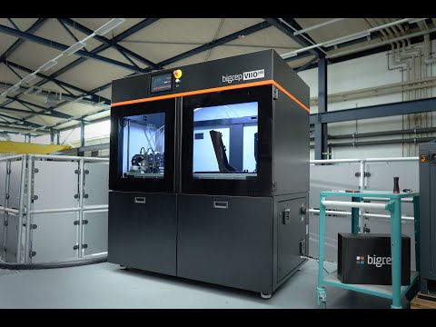
Simultaneously, 3D nanoprinting technologies are moving from research labs to industrial deployment. Two-photon polymerization (2PP) and focused electron/ion beam-induced deposition (FEBID/FIBID) are now being used to fabricate complex 3D nanostructures with feature sizes below 100 nm. Companies like Nanoscribe (a BICO company) have commercialized 2PP-based printers capable of producing intricate photonic, biomedical, and micro-optical components, with recent system upgrades supporting higher throughput and multi-material capabilities. These advances are enabling the direct fabrication of functional nanodevices, such as micro-robots and lab-on-chip systems, with unprecedented geometric freedom.
In parallel, bottom-up approaches such as template-assisted self-assembly and directed self-assembly (DSA) are being integrated into semiconductor manufacturing flows. Intel and TSMC have both reported progress in leveraging DSA for sub-10 nm patterning, reducing reliance on extreme ultraviolet (EUV) lithography and lowering process costs. These methods harness the intrinsic ordering of block copolymers or nanoparticles to define device features, offering scalability and defect reduction.
Looking ahead, the next few years are expected to see further convergence of these techniques. Hybrid fabrication platforms that combine ALD, 3D nanoprinting, and self-assembly are under active development, aiming to unlock new device architectures for quantum computing, neuromorphic hardware, and advanced photonics. The integration of in-situ metrology and AI-driven process control is anticipated to further enhance yield and reproducibility. As these breakthroughs mature, the nanodevice fabrication ecosystem—anchored by innovators like ASM International, Lam Research, Nanoscribe, Intel, and TSMC—is poised to deliver devices with functionalities and complexities previously unattainable, heralding a new era in nanoelectronics and nanomedicine.
Material Innovations: Graphene, 2D Materials, and Beyond
The landscape of advanced nanodevice fabrication is being rapidly transformed by material innovations, particularly the integration of graphene, other two-dimensional (2D) materials, and emerging heterostructures. As of 2025, these materials are enabling new device architectures with unprecedented electrical, optical, and mechanical properties, driving progress in sectors such as semiconductors, flexible electronics, and quantum technologies.
Graphene, a single layer of carbon atoms arranged in a hexagonal lattice, remains at the forefront due to its exceptional carrier mobility, mechanical strength, and thermal conductivity. Companies like Graphenea and 2D Semiconductors are supplying high-quality graphene and related 2D materials, supporting both research and commercial prototyping. In 2025, wafer-scale synthesis and transfer techniques have matured, with Graphenea offering CVD-grown graphene on 200 mm wafers, a critical step for integration with standard semiconductor processes.
Beyond graphene, transition metal dichalcogenides (TMDs) such as MoS2 and WS2 are gaining traction for their intrinsic bandgaps, making them suitable for logic and optoelectronic devices. 2D Semiconductors and Sixonia Tech are notable suppliers, providing monolayer and few-layer TMDs tailored for device fabrication. Recent advances in deterministic transfer and stacking methods have enabled the creation of van der Waals heterostructures, where different 2D materials are layered to engineer bespoke electronic and photonic properties.
In parallel, the development of scalable, contamination-free fabrication processes is a key focus. Companies such as Oxford Instruments are delivering atomic layer deposition (ALD) and plasma etching tools optimized for 2D materials, addressing challenges in uniformity and interface quality. These process innovations are crucial for the reliable production of nanodevices such as field-effect transistors (FETs), photodetectors, and sensors.
Looking ahead, the next few years are expected to see the commercialization of 2D material-based devices in niche applications, including high-frequency electronics, flexible displays, and biosensors. Collaborative efforts between material suppliers, tool manufacturers, and device integrators are accelerating the transition from laboratory-scale demonstrations to pilot production. As the ecosystem matures, the integration of 2D materials with silicon CMOS and the exploration of novel materials beyond graphene—such as borophene and phosphorene—are poised to further expand the capabilities of advanced nanodevice fabrication.
Leading Players and Strategic Partnerships (e.g., intel.com, ibm.com, imec-int.com)
The landscape of advanced nanodevice fabrication in 2025 is defined by a dynamic interplay among leading semiconductor manufacturers, research institutes, and strategic alliances. As device dimensions approach the sub-2 nm regime, the complexity of fabrication processes has necessitated unprecedented collaboration and investment.
Among the foremost players, Intel Corporation continues to spearhead innovation in transistor architecture and process technology. In 2024, Intel announced progress on its 18A process node, leveraging RibbonFET gate-all-around transistors and PowerVia backside power delivery, with pilot production slated for 2025. These advancements are critical for enabling denser, more energy-efficient nanodevices, and Intel’s foundry services are increasingly open to external customers, fostering ecosystem partnerships.
IBM remains a pivotal force in nanodevice R&D, particularly through its Albany Nanotech Complex. In 2023, IBM, in collaboration with Samsung Electronics, demonstrated the world’s first 2 nm nanosheet transistor technology, promising up to 45% improved performance or 75% lower energy use compared to 7 nm nodes. IBM’s open innovation model, involving academic and industrial partners, is expected to accelerate the commercialization of sub-2 nm devices by 2025 and beyond.
European research hub imec is central to global nanodevice fabrication efforts, acting as a bridge between academia and industry. Imec’s pilot lines in Leuven, Belgium, are equipped for advanced EUV lithography and atomic layer deposition, supporting collaborative projects with leading chipmakers and equipment suppliers. In 2024, imec launched its Sustainable Semiconductor Technologies and Systems (SSTS) program, uniting over 70 partners to address the environmental impact of next-generation nanofabrication.
Strategic partnerships are increasingly vital. For example, Taiwan Semiconductor Manufacturing Company (TSMC) and ASML have deepened their collaboration on high-NA EUV lithography, a cornerstone for sub-2 nm device production. TSMC’s roadmap includes mass production of 2 nm chips in 2025, leveraging ASML’s latest EUV systems. Meanwhile, Samsung Electronics is advancing its Gate-All-Around (GAA) transistor technology, with plans for 1.4 nm node development in the coming years.
Looking ahead, the convergence of expertise from these industry leaders and research consortia is expected to drive breakthroughs in nanodevice fabrication, with a focus on scaling, energy efficiency, and sustainability. The next few years will likely see intensified cross-border partnerships, shared pilot lines, and co-development of new materials and process technologies, shaping the future of nanoelectronics.
Applications: Electronics, Healthcare, Energy, and Emerging Sectors
Advanced nanodevice fabrication is rapidly transforming multiple sectors, with 2025 marking a pivotal year for both commercial deployment and research breakthroughs. In electronics, the continued miniaturization of transistors and memory devices is being driven by innovations in atomic layer deposition, extreme ultraviolet (EUV) lithography, and advanced patterning. Leading semiconductor manufacturers such as Intel Corporation and Taiwan Semiconductor Manufacturing Company (TSMC) are pushing the boundaries of logic and memory scaling, with sub-2nm process nodes expected to enter pilot production. These advances enable higher performance and energy efficiency in consumer electronics, data centers, and AI accelerators.
In healthcare, nanodevice fabrication is enabling the development of highly sensitive biosensors, implantable devices, and targeted drug delivery systems. Companies like Thermo Fisher Scientific are leveraging nanofabrication techniques to produce next-generation diagnostic platforms capable of detecting biomarkers at ultra-low concentrations, facilitating early disease detection and personalized medicine. Additionally, the integration of nanostructured materials in wearable health monitors is improving real-time physiological monitoring, with several startups and established firms advancing towards regulatory approvals and commercial launches in 2025.
The energy sector is witnessing the integration of nanodevices in advanced battery technologies, solar cells, and energy harvesting systems. Samsung Electronics and Panasonic Corporation are actively developing nanostructured electrodes and solid-state battery components, aiming to enhance energy density, charging speed, and safety. In photovoltaics, nanofabrication is enabling the production of perovskite and tandem solar cells with record efficiencies, with pilot lines and demonstration projects expected to scale up in the next few years.
Emerging sectors such as quantum computing and neuromorphic engineering are also benefiting from advanced nanodevice fabrication. IBM and Intel Corporation are fabricating quantum dots, superconducting circuits, and memristive devices at the nanoscale, which are essential for the realization of scalable quantum processors and brain-inspired computing architectures. The next few years are anticipated to see increased collaboration between industry and academia, as well as the establishment of dedicated nanofabrication foundries to accelerate prototyping and commercialization.
- Electronics: Sub-2nm logic and memory devices, AI hardware accelerators
- Healthcare: Ultra-sensitive biosensors, implantable nanodevices, wearable monitors
- Energy: Nanostructured batteries, advanced solar cells, energy harvesting
- Emerging: Quantum computing, neuromorphic chips, next-gen sensors
Overall, 2025 and the following years are set to witness significant advancements in nanodevice fabrication, with broad implications for performance, efficiency, and new functionalities across electronics, healthcare, energy, and emerging technology sectors.
Regulatory Landscape and Industry Standards (e.g., ieee.org, semiconductors.org)
The regulatory landscape and industry standards for advanced nanodevice fabrication are rapidly evolving in 2025, reflecting both the accelerating pace of technological innovation and the growing need for harmonized global frameworks. As nanodevices become increasingly central to sectors such as semiconductors, healthcare, and quantum computing, regulatory bodies and industry consortia are intensifying efforts to ensure safety, interoperability, and quality across the supply chain.
A cornerstone of standardization in this field is the work of the IEEE, which continues to update and expand its suite of standards relevant to nanotechnology and nanoelectronics. The IEEE Nanotechnology Council, for example, is actively developing guidelines for the characterization, testing, and reliability assessment of nanoscale devices, with new working groups focusing on topics such as nanomaterial integration and device modeling. These standards are critical for ensuring that devices fabricated at the nanoscale meet rigorous performance and safety benchmarks, facilitating both commercial adoption and regulatory compliance.
In parallel, the SEMI organization, a global industry association representing the electronics manufacturing and design supply chain, is playing a pivotal role in shaping process and equipment standards for nanodevice fabrication. SEMI’s International Standards Program, which brings together stakeholders from across the semiconductor ecosystem, has recently prioritized the development of protocols for contamination control, defect inspection, and advanced lithography—areas that are particularly challenging at the nanoscale. These efforts are expected to culminate in new or revised standards over the next few years, directly impacting how manufacturers design and operate their fabrication facilities.
On the regulatory front, agencies such as the U.S. Food and Drug Administration (FDA) and the European Medicines Agency (EMA) are increasingly engaged in the oversight of nanodevices, especially those intended for medical or diagnostic applications. These agencies are collaborating with industry and academic experts to refine guidance documents that address the unique properties and risks associated with nanoscale materials and devices. For instance, the FDA’s Nanotechnology Task Force is expected to release updated recommendations in 2025, focusing on premarket evaluation and post-market surveillance of nanodevice-enabled products.
Looking ahead, the convergence of industry-driven standards and regulatory frameworks is anticipated to accelerate the safe and reliable commercialization of advanced nanodevices. Ongoing collaboration between organizations such as IEEE, SEMI, and regulatory agencies will be essential in addressing emerging challenges, including ethical considerations, environmental impact, and cross-border harmonization. As the field matures, these coordinated efforts are likely to set the foundation for robust global governance of nanodevice fabrication through the remainder of the decade.
Supply Chain, Manufacturing Challenges, and Solutions
The supply chain and manufacturing landscape for advanced nanodevice fabrication in 2025 is characterized by both significant challenges and innovative solutions, as the industry strives to meet the demands of next-generation electronics, quantum devices, and biomedical applications. The complexity of nanodevice architectures—often involving sub-5 nm features, heterogeneous integration, and novel materials—places unprecedented pressure on supply chains, equipment manufacturers, and material suppliers.
A primary challenge is the sourcing and purity of advanced materials such as high-k dielectrics, 2D materials (e.g., graphene, MoS2), and specialized photoresists. The need for atomic-level precision in deposition and etching processes has led to increased reliance on a small number of suppliers capable of delivering ultra-high-purity chemicals and substrates. For example, BASF and DuPont are among the few global chemical companies with the capacity to supply the specialty materials required for extreme ultraviolet (EUV) lithography and atomic layer deposition (ALD) processes.
Equipment availability and lead times remain a bottleneck, particularly for advanced lithography and metrology tools. ASML continues to be the sole supplier of EUV lithography systems, which are essential for fabricating the smallest device features. The company has reported record order backlogs in 2024 and 2025, with delivery times stretching up to two years for some systems, reflecting both surging demand and the complexity of the equipment. Similarly, Lam Research and Applied Materials are critical providers of etch and deposition tools, and have expanded their manufacturing capacity to address global shortages.
Geopolitical tensions and export controls, particularly between the US, China, and the EU, have further complicated the nanodevice supply chain. Restrictions on the export of advanced semiconductor manufacturing equipment and materials have prompted companies in China to accelerate domestic development of lithography and process tools, with firms like SMIC investing heavily in R&D and local supply chain partnerships.
To address these challenges, industry leaders are adopting several strategies. Multi-sourcing of critical materials, increased investment in supply chain transparency, and the establishment of regional manufacturing hubs are becoming standard. For instance, TSMC and Samsung Electronics are expanding their global footprint with new fabs in the US and Europe, aiming to reduce geographic risk and improve supply resilience. Additionally, digitalization and AI-driven supply chain management are being deployed to predict disruptions and optimize inventory.
Looking ahead, the outlook for advanced nanodevice fabrication is cautiously optimistic. While supply chain constraints and manufacturing challenges are expected to persist through 2026, ongoing investments in capacity, localization, and process innovation are likely to gradually alleviate bottlenecks, enabling the continued scaling and diversification of nanodevice technologies.
Investment Trends, M&A Activity, and Funding Outlook
The advanced nanodevice fabrication sector is experiencing robust investment momentum in 2025, driven by surging demand for next-generation electronics, quantum computing, and biomedical applications. Venture capital and corporate funding have accelerated, with a focus on startups and scale-ups developing novel nanofabrication techniques, materials, and device architectures. Strategic investments are increasingly targeting companies with proprietary processes for atomic layer deposition, extreme ultraviolet (EUV) lithography, and advanced patterning, as these are critical for sub-5nm and even sub-2nm device nodes.
Major semiconductor manufacturers such as Taiwan Semiconductor Manufacturing Company (TSMC), Samsung Electronics, and Intel Corporation have announced multi-billion-dollar capital expenditure plans through 2026, with significant allocations for expanding nanofabrication capabilities and R&D in advanced process nodes. For example, TSMC’s ongoing investments in its Arizona and Taiwan fabs are explicitly aimed at scaling up 2nm and below technologies, while Samsung is expanding its foundry operations in South Korea and the US to support advanced logic and memory devices. Intel’s IDM 2.0 strategy, meanwhile, includes both internal capacity expansion and external foundry services, with a strong emphasis on advanced packaging and nanofabrication.
Mergers and acquisitions (M&A) activity has intensified, particularly among equipment suppliers and materials innovators. In 2024 and early 2025, several notable deals have been completed or announced. ASML Holding, the world’s leading supplier of EUV lithography systems, has continued to invest in strategic partnerships and minority stakes in companies developing next-generation mask and metrology solutions. Applied Materials and Lam Research have both pursued acquisitions to strengthen their portfolios in atomic layer etching and advanced deposition, aiming to address the increasingly complex requirements of nanodevice fabrication.
On the funding front, government initiatives in the US, EU, and Asia are providing substantial incentives for domestic nanofabrication ecosystems. The US CHIPS and Science Act, for instance, is channeling billions into semiconductor R&D and manufacturing, with a portion earmarked for nanodevice innovation. The European Union’s Chips Act and similar programs in Japan and South Korea are fostering public-private partnerships and direct grants to accelerate the commercialization of advanced nanofabrication technologies.
Looking ahead, the funding outlook remains positive, with continued inflows expected from both private and public sources. The sector’s capital intensity and the race to achieve technological leadership at the atomic scale are likely to sustain high levels of investment, M&A, and strategic collaboration through at least 2027. This dynamic environment is expected to further consolidate the position of leading players while enabling the emergence of specialized startups focused on critical nanofabrication challenges.
Future Outlook: Disruptive Technologies and Market Opportunities Through 2030
The landscape of advanced nanodevice fabrication is poised for significant transformation through 2030, driven by disruptive technologies and expanding market opportunities. As of 2025, the sector is witnessing rapid advancements in both materials and manufacturing techniques, with a strong focus on scaling down device dimensions while enhancing performance and energy efficiency. Key players in the semiconductor and nanotechnology industries are investing heavily in next-generation fabrication processes, such as extreme ultraviolet (EUV) lithography, atomic layer deposition (ALD), and directed self-assembly (DSA), to push the boundaries of miniaturization and integration.
Leading semiconductor manufacturers, including Intel Corporation, Taiwan Semiconductor Manufacturing Company (TSMC), and Samsung Electronics, are at the forefront of implementing sub-2nm process nodes, with pilot production lines expected to ramp up between 2025 and 2027. These advancements are enabling the fabrication of transistors and memory devices with unprecedented density and speed, opening new possibilities for artificial intelligence, high-performance computing, and edge devices. For instance, TSMC has announced plans to commercialize its 2nm technology by 2025, leveraging nanosheet transistor architectures to overcome the limitations of traditional FinFET designs.
Beyond traditional silicon-based devices, the integration of novel materials such as 2D transition metal dichalcogenides (TMDs), graphene, and other atomically thin semiconductors is gaining momentum. Companies like IBM and Applied Materials are actively developing processes to incorporate these materials into next-generation logic and memory devices, aiming to achieve superior electrical properties and further reduce power consumption. The convergence of advanced materials with innovative fabrication techniques is expected to catalyze the emergence of flexible, wearable, and even implantable nanodevices, expanding the addressable market into healthcare, IoT, and consumer electronics.
In parallel, the adoption of advanced metrology and inspection tools is becoming critical to ensure yield and reliability at the nanoscale. Equipment suppliers such as ASML and Lam Research are introducing new solutions for in-line process control, defect detection, and atomic-level characterization, which are essential for high-volume manufacturing of nanodevices.
Looking ahead to 2030, the market for advanced nanodevice fabrication is expected to be shaped by continued innovation in quantum computing, neuromorphic engineering, and heterogeneous integration. Strategic collaborations between device manufacturers, materials suppliers, and equipment vendors will be crucial to overcoming technical challenges and accelerating commercialization. As the ecosystem matures, the proliferation of disruptive nanodevices is set to unlock new applications and revenue streams across multiple industries, positioning advanced nanofabrication as a cornerstone of the next technological era.
Sources & References
- IBM
- ASML Holding
- Thermo Fisher Scientific
- First Solar
- National Nanotechnology Initiative
- ASM International
- Nanoscribe
- 2D Semiconductors
- Sixonia Tech
- Oxford Instruments
- imec
- IEEE
- BASF
- DuPont
- SMIC